


 The Right Approach: I Hear the Train A Comin'
 It’s Only Common Sense: OCCAM—the Time Is Now
 Marcy's Musings: The Growing Industry
A-Laser Helps Cardica Produce Next-Generation Medical Devices
August 4, 2015 | A-LaserEstimated reading time: 2 minutes
Cardica, a designer and manufacturer of proprietary stapling and automated anastomotic devices for cardiac and laparoscopic surgical procedures, has partnered with precision laser-cutting and engineering firm, A-Laser, to expand and refine its line of next-generation medical devices.
“For several years, we have worked with A-Laser on a number of product prototypes as well as ongoing precision parts manufacturing,” explains Donovan Ware, Materials Manager for Redwood City, California-based Cardica. “The quality of the laser-cut components A-Laser supplies is consistently high and the engineering team continues to be an invaluable resource for ensuring proper materials sourcing and design collaboration.”
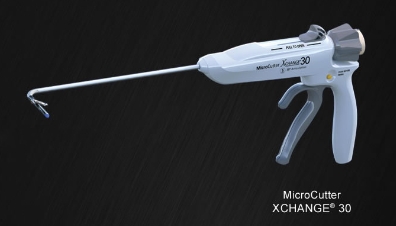
Cardica’s relationship with A-Laser began with the development of its revolutionary MicroCutter XCHANGE® 30 surgical stapler, an 80° articulating device with an exceptionally small 5mm shaft. Precision laser cutting of thin metal parts with tight tolerances was critical for the prototype development of this product and A-Laser’s comprehensive range of laser cutting services and the company’s engineering expertise have been instrumental in the progression of the MicroCutter product line.
“Our partnership with Cardica is very rewarding,” comments Josh Saunders, A-Laser’s President. “Knowing that we are playing a part in the manufacture of revolutionary medical devices is gratifying. And, the challenging designs from Cardica drive us to innovate new ways to manufacture exceptionally small, precise stainless steel components. In fact, one part can only be manufactured through a process of chemical etching and laser cutting, which is a technique A-Laser perfected and now employs to produce a specialty part used in Cardica’s MicroCutter device.”
In addition to its laser cutting expertise, A-Laser’s short lead times and local proximity are key advantages for Cardica. Reduced cycle times offer numerous benefits including improved productivity, shortened product development cycles, nimble design modification capability and inventory reduction, among others. “A-Laser is very responsive and goes above and beyond,” says Ware. “We can deliver a design and have parts in a couple of days. For a small company that’s trying to prototype very quickly, those days save us a huge amount of time and money. Our relationship with A-Laser continues to provide benefits on multiple fronts and, ultimately, we believe that surgeons and patients are the beneficiaries.”
About A-Laser, an FCT Companies Business
Based in Milpitas, California, A-Laser offers precision parts manufacturing for a variety of end markets including medical, industrial and electronics, among others. Integrating broad process capabilities such as laser marking, chemical etching, bending and forming and CO 2 laser cutting, A-Laser is delivering innovative products that address complex design requirements. A pioneer in the laser direct structuring (LDS) process, A-Laser technologists have revolutionized the molded interconnect device (MID) market and are providing customers with limitless design and production opportunities. For more information, visit www.a-laser.com.
Share on:


Suggested Items
Cadence, TSMC Collaborate on Wide-Ranging Innovations to Transform System and Semiconductor Design
04/25/2024 | Cadence Design SystemsCadence Design Systems, Inc. and TSMC have extended their longstanding collaboration by announcing a broad range of innovative technology advancements to accelerate design, including developments ranging from 3D-IC and advanced process nodes to design IP and photonics.
Ansys, TSMC Enable a Multiphysics Platform for Optics and Photonics, Addressing Needs of AI, HPC Silicon Systems
04/25/2024 | PRNewswireAnsys announced a collaboration with TSMC on multiphysics software for TSMC's Compact Universal Photonic Engines (COUPE). COUPE is a cutting-edge Silicon Photonics (SiPh) integration system and Co-Packaged Optics platform that mitigates coupling loss while significantly accelerating chip-to-chip and machine-to-machine communication.
Siemens’ Breakthrough Veloce CS Transforms Emulation and Prototyping with Three Novel Products
04/24/2024 | Siemens Digital Industries SoftwareSiemens Digital Industries Software launched the Veloce™ CS hardware-assisted verification and validation system. In a first for the EDA (Electronic Design Automation) industry, Veloce CS incorporates hardware emulation, enterprise prototyping and software prototyping and is built on two highly advanced integrated circuits (ICs) – Siemens’ new, purpose-built Crystal accelerator chip for emulation and the AMD Versal™ Premium VP1902 FPGA adaptive SoC (System-on-a-chip) for enterprise and software prototyping.
Listen Up! The Intricacies of PCB Drilling Detailed in New Podcast Episode
04/25/2024 | I-Connect007In episode 5 of the podcast series, On the Line With: Designing for Reality, Nolan Johnson and Matt Stevenson continue down the manufacturing process, this time focusing on the post-lamination drilling process for PCBs. Matt and Nolan delve into the intricacies of the PCB drilling process, highlighting the importance of hole quality, drill parameters, and design optimization to ensure smooth manufacturing. The conversation covers topics such as drill bit sizes, aspect ratios, vias, challenges in drilling, and ways to enhance efficiency in the drilling department.
Elevating PCB Design Engineering With IPC Programs
04/24/2024 | Cory Blaylock, IPCIn a monumental stride for the electronics manufacturing industry, IPC has successfully championed the recognition of the PCB Design Engineer as an official occupation by the U.S. Department of Labor (DOL). This pivotal achievement not only underscores the critical role of PCB design engineers within the technology landscape, but also marks the beginning of a transformative journey toward nurturing a robust, skilled workforce ready to propel our industry into the future.